Researchers in China produce Ultra stable Semiconductor using Henniker HPT-100
2D materials, are crystalline solids consisting of a single layer of atoms. These materials have unique properties due to their thickness being limited in one dimension, which makes them ideal for various applications including optoelectronics, energy generation, and high-performance composites. As an example, the most widely studied 2D material, graphene, has exceptional conductivity and is stronger than steel.
Another type of 2D material, violet phosphorus (2D-VP), is made up entirely of the element phosphorus. Due to its unique physical and electronic structure, it displays several highly sought-after properties such as a tuneable, large direct bandgap, a high charge carrier mobility, and a large optical absorption. This makes it ideal for realising optoelectronic devices for sensing, emitting, and controlling light.
Despite these interesting properties, violet phosphorus suffers from limited stability under ambient conditions. If handled in regular conditions, the material slowly degrades due to reactions with the oxygen in our atmosphere. Once this has happened, all the interesting properties disappear. This makes it difficult to integrate 2D-VP into useful devices.
Researchers at Shanghai Jiao Tong University (SJTU), led by Prof. Siyu Liu & Prof. Yanming Wang, were determined to find a solution to this stability issue. Using complex computational quantum simulations, the team of researchers discovered that the key to improving the stability of 2D-VP was to add a small amount of nitrogen to the material, a process called doping. Now that they knew what they needed to do, the team decided that plasma treatment would be the way to achieve this.

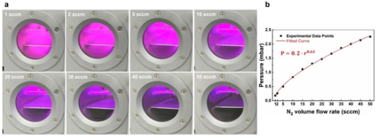
[1] Figure 1 - Researchers used the HPT-100 plasma system, which has fine control of the process pressure via the digitally controlled mass flow controller. Image courtesy of DOI: 10.1021/acsnano.4c09083
We asked the lead author of the paper, Mr Qingyuan He, why they chose plasma treatment:
"The choice of nitrogen plasma treatment for doping VP is based on the following considerations:
(1) Vacuum Environment: Few-layer VP flakes are highly susceptible to oxidation when exposed to air, leading to degradation. The plasma treatment is conducted in a vacuum environment, preventing direct contact between the VP flakes and oxygen, as well as minimizing the risk of other forms of contamination.
(2) Dual Function of Plasma Treatment: The nitrogen plasma treatment process involves physical etching and chemical doping. By carefully adjusting the relative strength of these two interactions, we can first achieve atomic-level flatness on the VP surface through physical etching, followed by the controlled introduction of nitrogen atoms via chemical doping. This combination results in a smooth surface, with reduced active sites, along with nitrogen doping, which is essential for significantly improving the stability of VP nanosheets.
(3) Practical Advantages: The plasma treatment process is simple, efficient, gentle, and highly scalable."
Despite plasma treatment being so well suited to the task, the team of researchers needed to carefully optimise the process to achieve the atomic-level flatness and correct doping of nitrogen into the 2D-VP.
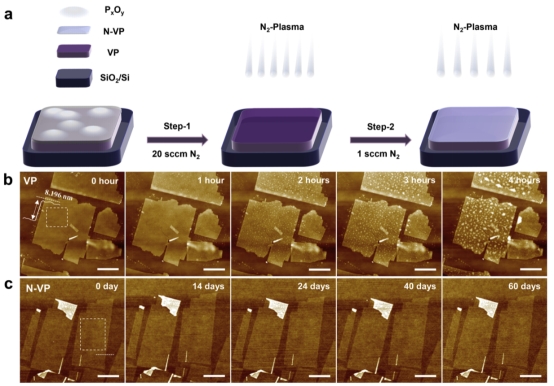
Using the fine pressure control available on their HPT-100 plasma system, it was discovered that a two-step plasma process was needed to achieve both the required flatness and the required doping.

[1] Figure 2 - Researchers used the HPT-100 plasma system, which has fine control of the process pressure via the digitally controlled mass flow controller. Image courtesy of DOI: 10.1021/acsnano.4c09083
In the first step, a higher plasma pressure is achieved by adjustment of the flow rate on the HPT-100 to 20sccm. This step removes the surface oxidation and etches the sample in a controlled manner to achieve an atomically flat surface.
For the second step, the flow rate is dropped to 1sccm, which reduces the plasma pressure whilst also giving individual nitrogen atoms more energy, allowing for steady doping of the 2D-VP. This generates the ultrastable N-VP (nitrogen doped violet phosphorus).
Using atomic force microscopy, the researchers showed that after this two-step process, the N-VP kept its flatness over a period of at least 60 days while regular 2D-VP would be degraded in a matter of a few hours. This achievement opens the possibility that N-VP can be usefully integrated into real world device without complex encapsulation or environmental controls.

[1] Figure 3 - d) The roughness of native VP increases over time due to degradation e) The roughness of nitrogen-doped VP remains very low even after 60 days f) Nitrogen doped VP remains. Image courtesy of DOI: 10.1021/acsnano.4c09083
This publication proves that plasma processing is key to controlling the surface properties of materials, in a controlled, scalable, and efficient manner. Other demonstrations by the group already show that this process also works on other 2D materials such as black phosphorus, and there is potential for it to help with others such as the transition metal dichalcogenides (i.e. MoS2, WSe2).
Original:
Researchers in China produce Ultra stable Semiconductor using Henniker HPT-100 - Henniker Plasma
References:
Thank you to the valuable contributions and discussions with Prof. Siyu Liu, Prof. Yanming, and Mr Qingyuan He.
Readers are referred to the original print, available through the provided DOI link, or click the link below for further details on the Henniker Plasma HPT-100.
[1] Highly Air-Stable N-Doped Two-Dimensional Violet Phosphorus with Atomically Flat Surfaces | ACS Nano
Qingyuan He, Dan-Dong Wang, Haixin Qiu, Nan Si, Qinglin Yuan, Rui Wang, Siyu Liu, and Yanming Wang
ACS Nano 2025 19 (1), 427-438
DOI: 10.1021/acsnano.4c09083


 LIST
LIST


